Nano-x Imaging Ltd has reportedly opened its new fabrication plant in South Korea to make semiconductor chips for the 3D medical imaging system Nanox.ARC system.
The plant has opened on schedule, is fully operational, and will produce Nanox.SOURCE, the Nanox MEMs (micro-electro-mechanical systems) that generate the digital X-ray source for Nanox.ARC system, which is capable of democratizing relevant access to imaging that is currently unavailable to nearly two-thirds of the world.
Nanox anticipates attaining the desired production scale by mid-2022. In addition, the company has been developing its production line abilities and setting up a functional assembly line at its Israeli plant to allow the desired scaling of production and preparation of shipping Nanox.ARC system.
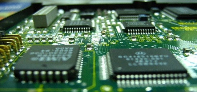
The new plant is a highly advanced fab facility, committed to the production of MEMs. Strategically situated next to the largest semiconductor cluster in the world in Yongin, South Korea, Nanox plant spans nearly 12,000 sq. mt., including a MEMs cleanroom spanning 1,200 sq. mt.
The core licensed technology of the company is a shift from an analog X-ray tube, which is like an LED (light-emitting diode) source. It has an on-off toggling feature developed to reduce the time of every operation. As the X-ray digital source maintains a low temperature, there is no electron-associated heat exiting the chip in comparison to analog X-ray sources. The expected X-ray tube range is 20-120 KV and it is light in weight and small.
Nanox is developing an end-to-end, holistic medical imaging solution that consolidates teleradiology services, AI medical imaging technology, and Nanox.ARC. While it continues the latest integration of the USARAD, Nanox.AI, and MDW acquisitions, the company believes these acquisitions will improve the services offered by the Nanox solution.
The plant is developed to conduct advanced practices of semiconductor fabrication, including 200nm photolithography using a KrF (krypton fluoride) scanner, physical vapor deposition (PVD) and chemical vapor deposition (CVD) of thin films, electrochemical metal etching, dry etching, C-module packaging for X-ray tubes, as well as chip inspection, and testing in vacuum, wet and chemical etching.
Source credit: